The world of semiconductor manufacturing has long been governed by one overarching principle: smaller, faster, more efficient. For decades, the industry has relentlessly pursued the miniaturisation of electronic components, riding the wave of Moore’s Law to double the number of transistors on a chip approximately every two years. ASML, a relatively obscure name outside the semiconductor sector, has been pivotal in this quest. Over the past 20 years, ASML’s development of extreme ultraviolet (EUV) lithography has been a journey fraught with technical challenges, skepticism, and massive financial bets. Today, it stands as a key enabler of the most sophisticated chips in the market, including Apple’s cutting-edge 3nm chips in the latest M3 processors.
The Rise of EUV Lithography
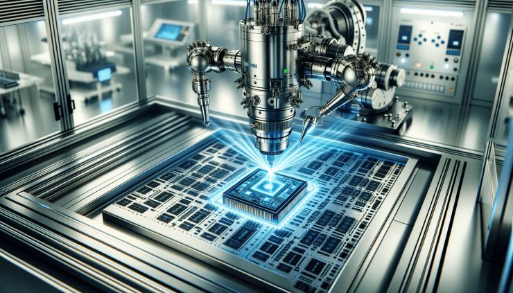
Lithography, the process of etching patterns on silicon to create integrated circuits, has historically used deep ultraviolet (DUV) light. However, as the demand for smaller transistors grew, the wavelengths of light used in the process became a limiting factor. Enter ASML’s EUV lithography, which uses a significantly shorter wavelength of 13.5 nanometers. This advancement permits the creation of circuits just a few nanometers across, pushing the boundaries of what’s possible in silicon.
The development of EUV technology by ASML was nothing short of a Herculean task. The journey began in the early 2000s, with the company investing heavily in research and development, despite widespread skepticism about the technology’s viability. EUV lithography required not only a new type of light source but also new materials for the masks and mirrors essential to the process, as well as an entirely new infrastructure for chip fabrication.
The challenges were monumental: the light source had to be incredibly intense, the optics had to be flawless to prevent any loss of the precious photons, and the entire apparatus had to operate in a vacuum to prevent the EUV light from being absorbed by air. It took years of collaboration with physicists, chemists, and engineers to surmount these obstacles.
The M3 Processor and the Mass Consumption Shift
ASML’s perseverance paid off. Fast forward to the present day, and EUV lithography has become the linchpin in the production of advanced chips, such as those found in Apple’s M3 processors. The transition to chips with a 3nm process, made possible by EUV lithography, signifies a monumental leap in computing power and efficiency.
With the advent of the M3 processors, Apple is once again at the forefront of personal computing technology, promising to bring unprecedented performance and energy efficiency to consumer products. This leap forward is not just about speed; it’s about the proliferation of high-powered computing in everyday devices, making advanced AI, augmented reality, and other sophisticated applications more accessible to the masses.
What This Means for Humanity
The implications of mass-produced 3nm chips are profound. As these advanced processors become more widely available, the cost per transistor plummets, and the possibility of integrating powerful computing capabilities into virtually anything becomes a reality. This democratisation of computing power could lead to a new wave of innovation in fields such as medicine, where complex simulations and data analysis can be conducted at speeds previously unimaginable.
Furthermore, the energy efficiency of these chips heralds a greener future for computing. Data centres, which are notorious for their high energy consumption, can achieve more while using less power, reducing the carbon footprint of cloud services that our modern digital lives rely on.
The Future of Computing
Looking ahead, ASML’s EUV lithography is poised to remain at the heart of semiconductor manufacturing. With the relentless push toward even smaller geometries, the company is already looking toward high-NA (numerical aperture) EUV systems, which promise to resolve features down to 1nm and beyond.
The journey of ASML and its EUV lithography is a testament to human ingenuity and persistence. From an ambitious idea to a crucial component in the most advanced chips, the 20-year odyssey of EUV lithography has not only reshaped the semiconductor industry but also set the stage for the next era of computing. As we stand on the brink of what some are calling the “post-Moore’s Law” age, it’s clear that the innovation brought forth by ASML will continue to shape the landscape of technology and propel humanity toward an increasingly interconnected and intelligent future.

Leave a comment